
A watch brand founder flew to Shenzhen last year to visit the factory coating his watch cases. He’d specified “PVD gold coating” on his purchase order. The factory said yes, no problem, PVD gold coating. When the first production batch arrived at his US warehouse, the gold color was beautiful. Rich, warm, exactly what he wanted.
Four months later, his early customers started posting photos on social media. The gold coating on the case backs was wearing through to silver steel underneath. Crown edges showed bare metal. The lugs where the strap attached had visible wear lines. His $299 watches looked like $30 fakes after four months of normal wear.
The problem wasn’t that the factory lied about using PVD. They did use PVD. The problem was which type of PVD coating they used and how they applied it. They used basic thermal evaporation with a coating thickness of 0.2 microns. For a watch case that experiences daily friction, impact, and skin contact, that combination guarantees premature wear. He needed arc ion plating at 0.8-1.2 microns minimum. But he never specified the PVD method or thickness in his order. He just wrote “PVD gold” and assumed the factory would choose appropriately.
They chose the cheapest option. Factories always choose the cheapest option when you don’t specify otherwise.
Understanding the different types of PVD coating isn’t academic knowledge reserved for materials engineers. It’s practical knowledge that determines whether your coated products last years or months. Whether your customers praise the durability or post complaint videos. Whether your brand builds a reputation for quality or becomes another cautionary tale about sourcing products from China without adequate specifications.
Table of Contents
| 1 | What PVD Coating Actually Is (The 60-Second Version) |
| 2 | Why Types of PVD Coating Matter for Your Product |
| 3 | Type 1: Magnetron Sputtering |
| 4 | Type 2: Arc Ion Plating (Cathodic Arc Deposition) |
| 5 | Type 3: Electron Beam Evaporation |
| 6 | Type 4: Thermal Evaporation |
| 7 | Type 5: Pulsed Laser Deposition |
| 8 | Type 6: Ion Beam Assisted Deposition (IBAD) |
| 9 | Type 7: High Power Impulse Magnetron Sputtering (HiPIMS) |
| 10 | PVD Coating Types Comparison Chart |
| 11 | Which PVD Type for Which Product Category |
| 12 | How Factories Cut Corners on PVD Coating |
| 13 | How to Specify PVD Coating in Your Production Orders |
| 14 | FAQ |
What PVD Coating Actually Is (The 60-Second Version)
PVD stands for Physical Vapor Deposition. The process works like this: inside a vacuum chamber, a solid source material (called the “target”) is converted into vapor through physical means (heat, electrical arc, ion bombardment, or laser energy). This vapor travels through the vacuum and deposits atom-by-atom onto your product’s surface, building up an extremely thin but extremely hard coating layer.
The result is a coating that’s physically bonded to the substrate at the atomic level. Not painted on. Not electroplated in a chemical bath. Physically deposited atom by atom in a vacuum environment. This atomic-level bonding is why PVD coatings are harder, more durable, and more resistant to wear than traditional plating methods.
Every PVD coating shares these characteristics: applied in a vacuum chamber, deposited from a vaporized solid source, builds up atom by atom, creates coatings typically 0.2-5 microns thick, and produces extremely hard surfaces (often harder than the substrate material itself).
What differs between the types of PVD coating is HOW the source material gets vaporized. That difference in vaporization method determines coating density, adhesion strength, surface smoothness, deposition rate, cost, and ultimately how long the coating lasts on your product.
Why Types of PVD Coating Matter for Your Product
A client once asked me why she should care about PVD methods. “Just tell the factory to make it gold and durable,” she said. I explained it this way:
Imagine you need to paint a wall. You could use a spray can, a roller, a brush, an airless sprayer, or an electrostatic gun. Each method puts paint on the wall. But the finish quality, coverage uniformity, thickness control, and durability differ dramatically between methods. You wouldn’t spray-paint a luxury car with a rattle can. You wouldn’t use an industrial electrostatic system to touch up a picture frame.
PVD coating types work the same way. Each method deposits material onto your product’s surface, but the quality characteristics of that deposit vary enormously. The wrong method for your application produces coatings that peel, wear through prematurely, show color inconsistency, or fail adhesion testing. The right method produces coatings that outlast the product itself.
For anyone involved in product development of coated metal products, understanding these differences prevents the exact scenario that destroyed my watch brand client’s first production run.
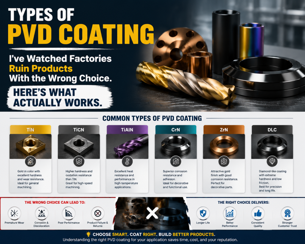
Type 1: Magnetron Sputtering
Magnetron sputtering is the most widely used PVD method for consumer products. If your factory says “PVD coating” without specifying the method, there’s a good chance they’re using magnetron sputtering. It’s versatile, produces good quality coatings, and the equipment is relatively affordable (by PVD standards).
How it works: A target material (titanium, chromium, zirconium, or other metals) sits inside the vacuum chamber. Argon gas is introduced. A strong magnetic field and electrical voltage ionize the argon atoms, creating a plasma. These energized argon ions slam into the target material, physically knocking atoms off its surface (this is the “sputtering”). The knocked-off atoms travel through the vacuum and deposit onto your product.
To create colors, reactive gases are introduced during sputtering. Nitrogen gas creates nitride compounds (titanium nitride produces gold color). Oxygen creates oxide compounds. Carbon-containing gases create carbide compounds. By controlling which reactive gas is present and in what quantity, the factory controls the coating color.
Coating characteristics:
Density: Good. Sputtered coatings are reasonably dense with few voids or pinholes.
Adhesion: Good to excellent when substrate is properly prepared (cleaned, sometimes ion-etched before coating).
Surface smoothness: Excellent. Magnetron sputtering produces very smooth coatings without the “macro-particle” defects common in arc processes. This makes it ideal for decorative applications where surface appearance matters.
Thickness uniformity: Good. The magnetic field helps distribute the sputtered atoms relatively evenly across the product surface.
Deposition rate: Moderate. Slower than arc ion plating, which means longer cycle times and higher per-unit cost for thick coatings.
Common coating materials via magnetron sputtering:
| Titanium + Nitrogen | Titanium Nitride (TiN) | Gold |
| Titanium + Carbon/Nitrogen | Titanium Carbonitride (TiCN) | Rose gold / bronze |
| Chromium + Nitrogen | Chromium Nitride (CrN) | Silver-grey |
| Zirconium + Nitrogen | Zirconium Nitride (ZrN) | Light gold |
| Titanium + Carbon | Diamond-Like Carbon (DLC) | Black |
| Chromium | Chromium | Bright chrome |
Best applications: Jewelry, watch cases, eyeglass frames, decorative hardware, bathroom fittings, door handles, and any product where surface smoothness and visual quality are priorities. The smooth coating surface means no post-coating polishing is needed, which saves manufacturing steps and cost.
Cost range (2026): $0.30-2.00 per unit for small consumer products (jewelry, small hardware). $2.00-8.00 per unit for larger items (watch cases, architectural fittings). Cost varies with coating thickness, batch size, and product geometry.
Limitations: Slower deposition rate means thicker coatings take longer and cost more. Adhesion, while good, isn’t quite as strong as arc ion plating for applications facing severe mechanical stress. Line-of-sight process means complex geometries with deep recesses may have thin spots where the sputtered atoms can’t reach easily.
Type 2: Arc Ion Plating (Cathodic Arc Deposition)
Arc ion plating produces the hardest, most durable PVD coatings available for consumer products. When maximum wear resistance matters more than perfect surface smoothness, arc ion plating is the method serious manufacturers choose.
How it works: A high-current electrical arc strikes the target material surface, creating an extremely hot spot (thousands of degrees) that vaporizes the target material explosively. Unlike sputtering’s gentle atom-by-atom removal, arc evaporation blasts material off the target in a highly energized plasma. These highly energized ions arrive at the product surface with significant kinetic energy, driving themselves into the substrate surface and creating exceptionally strong adhesion.
Coating characteristics:
Density: Excellent. The highest density of any standard PVD method. Virtually no voids or porosity in the coating structure.
Adhesion: Superior. The high-energy ion bombardment creates a graded interface between substrate and coating rather than an abrupt boundary. This graded interface resists delamination under mechanical stress better than any other PVD method.
Surface smoothness: Moderate. Arc evaporation produces “macro-particles” (tiny droplets of molten target material) that embed in the coating surface, creating microscopic bumps. For decorative applications requiring mirror-smooth surfaces, these macro-particles are a problem. For functional applications where hardness matters more than appearance, they’re acceptable.
Hardness: Highest of standard PVD methods. TiN coatings via arc plating typically measure 2400-2800 HV (Vickers hardness). The same TiN via sputtering measures 2000-2400 HV.
Deposition rate: Fast. Significantly faster than magnetron sputtering, meaning shorter cycle times and lower per-unit cost for thick coatings.
Best applications: Cutting tools, drill bits, industrial wear parts, watch cases for rugged/sport watches, military hardware, automotive components, and any product where coating durability under mechanical stress is the primary requirement. Many premium watch brands (particularly sport and dive watches) specify arc ion plating because the coating survives impacts and abrasion that would wear through sputtered coatings.
Cost range (2026): $0.50-3.00 per unit for small products. $3.00-12.00 for larger items. Despite faster deposition rates, arc equipment is more expensive to operate and maintain, partially offsetting the speed advantage.
Limitations: Macro-particle defects require post-coating polishing for decorative applications, adding a manufacturing step and cost. Not ideal for products requiring optical-quality surface finish without additional processing. The high-energy process can cause thermal stress on heat-sensitive substrates.
The factory choice dilemma: Many Chinese coating facilities own both sputtering and arc equipment. When you specify “PVD coating” without specifying the method, they’ll use whichever machine has available capacity or whichever is cheaper to run for your batch size. For products needing maximum durability (watches, tools, heavy-use hardware), explicitly specify “cathodic arc deposition” or “arc ion plating” in your product specifications.
Type 3: Electron Beam Evaporation
Electron beam (e-beam) evaporation uses a focused beam of high-energy electrons to heat and vaporize the target material. The electron beam melts a small area of the target in a crucible, creating vapor that rises and deposits on products positioned above.
How it works: An electron gun generates a beam of electrons that’s magnetically focused onto the target material sitting in a water-cooled crucible. The beam heats the target to its evaporation point. Vapor rises from the molten pool and deposits on substrates mounted above the source. The process happens in high vacuum (lower pressure than sputtering), producing very pure coatings.
Coating characteristics:
Density: Moderate. Lower than sputtering or arc methods because the depositing atoms arrive with less kinetic energy. The coating structure can contain columnar voids that reduce density.
Adhesion: Moderate. Without additional ion bombardment assistance, e-beam coatings have weaker adhesion than sputtered or arc-deposited coatings. Often combined with ion assist (becoming IBAD, covered later) to improve adhesion.
Surface smoothness: Excellent. No macro-particles. Very smooth, uniform coatings suitable for optical and decorative applications.
Deposition rate: High for certain materials. E-beam evaporation can deposit material quickly, making it cost-effective for thick coatings on large batches.
Purity: Excellent. The electron beam only heats the target material, not the crucible, minimizing contamination. Important for optical coatings and electronics applications.
Best applications: Optical coatings (anti-reflective coatings on lenses), thin-film electronics, decorative coatings on large flat surfaces, and applications where coating purity matters more than mechanical hardness. Less common for consumer hardware products but relevant for eyewear, optical instruments, and electronic device components.
Cost range (2026): $0.20-1.50 per unit for optical coatings on small components. $1.00-5.00 for larger decorative applications. Generally less expensive per unit than arc plating for thin decorative coatings.
Limitations: Lower adhesion without ion assist makes it unsuitable for products facing mechanical wear. Line-of-sight limitations are more pronounced than sputtering. Not the right choice for jewelry, watches, or hardware that experiences friction and impact.
Type 4: Thermal Evaporation
Thermal evaporation is the simplest and oldest PVD method. It’s also the cheapest. And in consumer product sourcing, “cheapest” often means “what the factory uses when you don’t specify otherwise.”
How it works: The target material is placed in a resistive heating element (typically a tungsten boat or filament) inside the vacuum chamber. Electrical current heats the element, which heats the target material until it evaporates. The vapor rises and deposits on products above. No plasma, no ion bombardment, no magnetic fields. Just heat and vacuum.
Coating characteristics:
Density: Low to moderate. Thermally evaporated coatings tend to be porous with columnar microstructure. This porosity makes them less protective and less durable than denser coatings from sputtering or arc methods.
Adhesion: Poor to moderate. Without energetic ion bombardment, the coating sits on the surface rather than being driven into it. Adhesion depends heavily on substrate cleanliness and surface preparation.
Surface smoothness: Good. No macro-particles. Smooth coatings suitable for decorative applications where durability isn’t critical.
Hardness: Lower than sputtering or arc methods for the same coating material. The porous structure reduces effective hardness.
Deposition rate: Moderate to high depending on material.
Best applications: Decorative coatings on products with minimal wear exposure (display items, packaging components, costume jewelry meant for limited wear). Reflective coatings on mirrors and optical components. Metallization of plastic parts for decorative purposes.
Cost range (2026): $0.10-0.80 per unit. The lowest cost of any PVD method. This is precisely why budget factories default to thermal evaporation when specifications don’t mandate a better method.
The sourcing warning: This is the method that destroyed my watch brand client’s first production run. Thermal evaporation produces coatings that look identical to arc-deposited coatings when new. Same gold color. Same visual appearance. But the coating is thinner, softer, less dense, and less adherent. It wears through in months instead of years. If your factory quotes PVD coating at suspiciously low prices, they’re likely using thermal evaporation. The cost savings come directly from your product’s durability. Specify the method explicitly and verify during quality inspection.
Type 5: Pulsed Laser Deposition (PLD)
Pulsed laser deposition uses high-energy laser pulses to ablate material from a target surface. Each laser pulse vaporizes a small amount of target material, creating a plasma plume that deposits on the substrate.
How it works: A high-power pulsed laser (typically excimer or Nd:YAG) fires through a window in the vacuum chamber and strikes the target material. Each pulse creates a tiny explosion of vaporized material that expands as a plasma plume toward the substrate. The process repeats at high frequency (10-50 pulses per second typically), building up the coating pulse by pulse.
Coating characteristics:
Density: Excellent. PLD produces some of the densest coatings achievable by any PVD method. The energetic plasma plume creates highly compact coating structures.
Adhesion: Very good. The energetic species in the plasma plume promote strong bonding to the substrate.
Composition control: Superior. PLD transfers the exact composition of the target material to the coating with minimal change. This makes it ideal for complex multi-element coatings where precise stoichiometry matters.
Surface smoothness: Variable. Depends on laser parameters. Can produce very smooth coatings or coatings with particulate defects depending on optimization.
Deposition rate: Low for large areas. PLD deposits material over a small area per pulse, making it slow for coating large products or large batches.
Best applications: Research and development. Specialized electronic and optical coatings. Superconductor thin films. Biomedical coatings. Rarely used for standard consumer product manufacturing due to slow deposition rates and high equipment costs. However, relevant for high-value medical devices, specialized sensors, and advanced electronics where coating composition precision justifies the cost.
Cost range (2026): $5.00-50.00+ per unit. Prohibitively expensive for most consumer products. Reserved for high-value specialized applications.
Relevance to product sourcing: Minimal for most consumer brands. If a factory claims to use PLD for your jewelry or hardware products, they’re either confused about terminology or misrepresenting their process. PLD is a laboratory and specialty manufacturing technique, not a production-scale consumer product coating method.
Type 6: Ion Beam Assisted Deposition (IBAD)
IBAD combines evaporation (thermal or e-beam) with simultaneous ion beam bombardment. While one source deposits coating material, a separate ion gun bombards the growing coating with energetic ions, compacting it and improving adhesion.
How it works: Two things happen simultaneously inside the vacuum chamber. An evaporation source (thermal or e-beam) deposits coating material onto the product. At the same time, an ion gun directs a beam of energetic ions (typically argon or nitrogen) at the product surface. These ions compact the growing coating, drive out voids, improve density, and enhance adhesion by mixing the coating/substrate interface at the atomic level.
Coating characteristics:
Density: Very good. The ion bombardment eliminates the porosity problems of standard evaporation, producing dense coatings approaching sputtering quality.
Adhesion: Very good. The ion mixing at the interface creates strong bonding that standard evaporation can’t achieve alone.
Surface smoothness: Good to excellent. Maintains the smooth surface quality of evaporation while adding the density benefits of ion bombardment.
Flexibility: High. By adjusting ion beam parameters independently from the evaporation source, operators can fine-tune coating properties (stress, density, composition) with precision not available in single-source methods.
Best applications: Optical coatings requiring both smoothness and durability. Anti-reflective coatings on premium eyewear. Protective coatings on precision instruments. Decorative coatings on products needing better durability than standard evaporation but smoother surfaces than arc plating.
Cost range (2026): $1.00-5.00 per unit for consumer products. More expensive than standard evaporation but less than arc plating for comparable durability. A middle-ground option that some premium eyewear and instrument manufacturers prefer.
Sourcing context: IBAD equipment is less common in Chinese coating facilities than sputtering or arc equipment. If you need IBAD specifically, verify that your factory actually has the dual-source setup required. Some facilities claim IBAD capability but actually run standard evaporation without the ion assist, producing inferior coatings at IBAD prices.
Type 7: High Power Impulse Magnetron Sputtering (HiPIMS)
HiPIMS represents the cutting edge of PVD technology. It’s magnetron sputtering pushed to extreme power levels in short pulses, producing coatings that combine sputtering’s smoothness with arc plating’s density and adhesion.
How it works: Standard magnetron sputtering runs at continuous moderate power. HiPIMS applies power in extremely short, extremely intense pulses (microseconds long, but at peak powers 100-1000x higher than standard sputtering). These intense pulses create a much denser plasma with a much higher percentage of ionized target atoms. More ionized atoms means more energetic deposition, which means denser, harder, better-adhered coatings.
Coating characteristics:
Density: Excellent. Approaching arc plating density without arc plating’s macro-particle problems.
Adhesion: Excellent. The high ionization fraction creates strong substrate bonding comparable to arc methods.
Surface smoothness: Excellent. Maintains sputtering’s inherent smoothness advantage. No macro-particles because there’s no arc.
Hardness: Very high. HiPIMS TiN coatings achieve hardness values between standard sputtering and arc plating.
Stress control: Superior. The pulsed nature allows precise control of coating stress, reducing the risk of coating delamination on complex geometries.
Best applications: Premium watches, luxury hardware, high-end architectural fittings, medical implants, and cutting tools where both surface quality AND durability must be maximized simultaneously. HiPIMS eliminates the traditional trade-off between “smooth but less durable” (sputtering) and “durable but rougher” (arc).
Cost range (2026): $2.00-10.00 per unit for consumer products. More expensive than standard sputtering due to specialized power supply equipment and slower effective deposition rates. But for premium products where coating quality directly affects brand perception and product longevity, the cost premium is justified.
Sourcing reality: HiPIMS equipment is still relatively rare in Chinese coating facilities. Most facilities in Shenzhen and Dongguan that serve the consumer product market operate standard sputtering and arc equipment. HiPIMS is more common in European and Japanese coating facilities serving the luxury watch and medical device industries. If you need HiPIMS quality, you may need to source coating services from specialized facilities rather than general-purpose coating shops. A sourcing partner with coating industry connections can identify facilities with genuine HiPIMS capability.
PVD Coating Types Comparison Chart
| Magnetron Sputtering | Good | Good-Excellent | Excellent | High | Moderate | $0.30-2.00 | Jewelry, decorative hardware |
| Arc Ion Plating | Excellent | Superior | Moderate | Highest | Fast | $0.50-3.00 | Watches, tools, heavy-wear items |
| E-Beam Evaporation | Moderate | Moderate | Excellent | Moderate | High | $0.20-1.50 | Optical coatings, electronics |
| Thermal Evaporation | Low-Mod | Poor-Mod | Good | Low-Mod | Moderate | $0.10-0.80 | Budget decorative, display items |
| Pulsed Laser (PLD) | Excellent | Very Good | Variable | High | Low | $5.00-50.00 | Research, medical, specialized |
| IBAD | Very Good | Very Good | Good-Excellent | Good-High | Moderate | $1.00-5.00 | Premium optics, instruments |
| HiPIMS | Excellent | Excellent | Excellent | Very High | Slow-Mod | $2.00-10.00 | Luxury watches, premium hardware |
Which PVD Type for Which Product Category
Choosing the right PVD type starts with understanding what your product faces in real-world use. Different products experience different stresses, and those stresses determine which coating characteristics matter most.
Jewelry (rings, bracelets, necklaces, earrings):
Rings and bracelets face constant friction, impact, and chemical exposure (hand soap, sanitizer, sweat). These need arc ion plating or HiPIMS with minimum 0.5 micron thickness for rings, 0.3 microns for necklaces and earrings that face less mechanical stress.
Earrings and necklaces face minimal mechanical wear but need excellent color consistency and smooth surfaces for visual appeal. Magnetron sputtering at 0.2-0.3 microns works well and costs less.
Watches:
Case and bracelet: Arc ion plating at 0.8-1.5 microns. These surfaces face daily impacts, desk diving scratches, and sleeve friction. Anything less than arc plating at adequate thickness wears through within a year of daily use.
Case back: Magnetron sputtering at 0.3-0.5 microns is adequate since case backs face less mechanical stress (protected by the wrist).
Crown and pushers: Arc ion plating at 1.0+ microns. These small components face concentrated finger pressure and rotational friction daily.
Kitchen and bathroom hardware:
Faucets and handles: Magnetron sputtering at 0.3-0.5 microns. These face moderate use but primarily need chemical resistance (cleaning products) and visual durability rather than impact resistance.
Cabinet pulls: Magnetron sputtering at 0.2-0.4 microns. Light use, primarily decorative function.
Cutting tools and industrial:
Arc ion plating at 2-5 microns. Maximum hardness and adhesion required. Surface smoothness is secondary to wear resistance. This is arc plating’s natural domain.
Eyewear frames:
IBAD or magnetron sputtering at 0.3-0.5 microns. Need smooth decorative finish plus moderate durability for daily handling. Arc plating’s macro-particles are unacceptable
on optical-quality surfaces where any surface irregularity is visible and distracting.
Architectural fittings (door handles, railings, elevator panels):
Magnetron sputtering or HiPIMS at 0.5-1.0 microns. These products face moderate mechanical stress but need long-term color stability under UV exposure and cleaning chemical contact. The larger surface areas make arc plating’s macro-particle defects more visible, favoring sputtering methods.
How Factories Cut Corners on PVD Coating (And What It Costs Your Brand)
I’ve seen every shortcut in the book during factory audits and quality inspections across coating facilities in Shenzhen, Dongguan, and Huizhou. Here are the most common ways factories reduce their coating costs at your product’s expense.
Shortcut #1: Reducing coating thickness below specification.
You specify 0.8 microns. The factory applies 0.3 microns. The product looks identical when new. The color is the same. The visual appearance is indistinguishable. But the thinner coating wears through in months instead of years. This is the single most common PVD quality issue in imported consumer products.
Why factories do it: Thinner coatings mean shorter cycle times in the vacuum chamber. Shorter cycles mean more batches per day. More batches mean more revenue from the same equipment. A factory running 0.3 micron cycles can process three times as many batches as one running 0.8 micron cycles on the same machine.
How to catch it: Require coating thickness measurement on sample pieces from every production batch. Calotest (ball crater test) is a simple, inexpensive method that measures coating thickness by grinding a small crater through the coating and measuring the crater geometry under a microscope. Specify this test in your quality control protocol. Any factory that refuses thickness verification is almost certainly running thin coatings.
Shortcut #2: Skipping substrate preparation.
Proper PVD coating requires meticulous substrate preparation. The product surface must be ultrasonically cleaned, degreased, and often ion-etched inside the vacuum chamber before coating begins. This preparation removes contaminants and creates a clean surface for atomic bonding.
Skipping or rushing preparation saves 15-30 minutes per batch. But coatings applied to contaminated surfaces have dramatically weaker adhesion. They peel, flake, or delaminate under stress that properly prepared coatings handle easily.
How to catch it: Adhesion testing. The cross-hatch tape test (ASTM D3359) scores the coating surface in a grid pattern, applies adhesive tape, and pulls it off. Properly adhered coatings show no removal. Poorly adhered coatings lift off with the tape. Require this test on samples from every batch.
Shortcut #3: Using thermal evaporation when arc or sputtering was specified.
Some facilities have multiple PVD systems. When the specified system is busy or down for maintenance, they run your products through whatever system is available. Thermal evaporation equipment is cheaper to operate and maintain, so it becomes the default when nobody is watching.
How to catch it: Hardness testing on coated samples. Arc-deposited TiN measures 2400-2800 HV. Sputtered TiN measures 2000-2400 HV. Thermally evaporated TiN measures 1500-2000 HV. A microhardness test immediately reveals which method was actually used, regardless of what the factory claims.
Shortcut #4: Overloading the chamber.
PVD chambers have optimal loading capacities. Overloading (cramming more products into each batch to increase throughput) creates shadowing effects where products block each other from the coating source. The result: uneven coating thickness across the batch. Products in the center get full thickness. Products on the edges or in shadowed positions get thin, incomplete coating that wears through prematurely.
How to catch it: Measure coating thickness on multiple pieces from different positions in the batch, not just one sample piece. If thickness varies more than 20% across samples from the same batch, the chamber was overloaded.
Shortcut #5: Inadequate vacuum level.
PVD requires high vacuum (typically 10^-3 to 10^-5 mbar) for quality coatings. Achieving and maintaining high vacuum takes time and well-maintained equipment. Leaky chambers, worn pump seals, or impatient operators who start coating before adequate vacuum is reached produce coatings contaminated with residual air molecules. These contaminated coatings have reduced hardness, poor adhesion, and inconsistent color.
How to catch it: Color consistency inspection across the batch. Contaminated coatings often show slight color variation (some pieces slightly different shade than others). Also, adhesion testing catches the weakened bonding that results from inadequate vacuum.
How to Specify PVD Coating in Your Production Orders
Your product specification sheet for PVD-coated products should include every one of these parameters. Leaving any of them unspecified gives the factory discretion to choose the cheapest option.
Required specifications:
PVD method: State explicitly which type (magnetron sputtering, cathodic arc deposition, HiPIMS, etc.). Don’t write “PVD” alone.
Coating material/compound: Specify the exact coating compound (TiN, TiCN, CrN, ZrN, DLC, etc.). Don’t write “gold color PVD” — specify “Titanium Nitride (TiN) via magnetron sputtering” or “Zirconium Nitride (ZrN) via cathodic arc.”
Coating thickness: State minimum acceptable thickness in microns. For example: “Minimum 0.8 microns TiN, measured via calotest on 3 random samples per batch.”
Color reference: Provide a physical color sample (a previously approved coated piece) or specify color coordinates (CIE Lab* values) with acceptable tolerance range. “Gold” means different things to different people and different factories. A physical reference or numerical color specification eliminates ambiguity.
Adhesion requirement: Specify the test method and pass criteria. For example: “Cross-hatch adhesion test per ASTM D3359, Classification 4B minimum (less than 5% coating removal).”
Hardness requirement: Specify minimum hardness if relevant for your application. For example: “Minimum 2200 HV microhardness measured on coated flat sample from same batch.”
Surface finish before coating: Specify the substrate surface condition required before PVD application. “Mirror polish to Ra 0.05 microns before coating” or “Brushed finish, 120-grit direction, before coating.”
Areas to coat: Clearly indicate which surfaces receive coating and which don’t. Use drawings with colored zones. Some products need full coating. Others need selective coating (exterior surfaces only, specific faces only). Unclear specifications result in either missed areas or wasted coating on hidden surfaces.
Masking requirements: If certain areas must remain uncoated (threading, mating surfaces, sensor windows), specify masking requirements explicitly.
Testing and verification requirements:
State which tests the factory must perform and document for each production batch. At minimum for consumer products:
Coating thickness measurement (calotest or ISO 20502 compliant method) on 3+ random samples per batch.
Adhesion test (cross-hatch tape test or scratch test per ASTM C1624) on 2+ samples per batch.
Color measurement (spectrophotometer reading) on 5+ samples per batch, compared against approved reference.
Visual inspection (100% of pieces) for coating defects: pinholes, flaking, discoloration, uncoated areas, macro-particle defects.
These test results should be documented and provided with each shipment. If a factory pushes back on testing requirements, that resistance tells you something important about their confidence in their own coating quality. Reputable coating facilities welcome verification because it demonstrates their quality to clients. Facilities cutting corners resist verification because it exposes their shortcuts.
PVD Coating vs. Electroplating: Why the Distinction Matters
Many product brands confuse PVD coating with electroplating or use the terms interchangeably. They’re fundamentally different processes with different performance characteristics. Understanding the distinction helps you specify correctly and evaluate factory claims accurately.
Electroplating deposits metal from a chemical solution using electrical current. The product is submerged in a bath containing dissolved metal ions. Electrical current causes those ions to deposit on the product surface. Common electroplated finishes include gold plating, nickel plating, chrome plating, and rhodium plating.
Key differences:
| Process environment | Vacuum chamber | Chemical bath |
| Bonding mechanism | Physical atomic deposition | Electrochemical deposition |
| Typical thickness | 0.2-5 microns | 0.5-25+ microns |
| Hardness | Very high (1500-3000 HV) | Low to moderate (200-900 HV) |
| Wear resistance | Excellent | Moderate |
| Environmental impact | Low (no chemical waste) | High (toxic bath chemicals) |
| Color options | Limited (gold, rose, black, grey, blue) | Wide (any platable metal color) |
| Cost per unit | Higher | Lower for thin decorative |
| Durability | Years of daily wear | Months to 1-2 years |
For products marketed as “tarnish-free” or “lifetime finish,” PVD coating is the defensible choice. Electroplating wears through faster, especially in thin decorative applications. However, electroplating offers thicker deposits and wider color options at lower cost, making it appropriate for products with shorter expected lifespans or less demanding use conditions.
When your factory offers “gold plating” at significantly lower cost than PVD, understand that you’re getting a softer, less durable finish that will wear through faster. That trade-off might be acceptable for fashion jewelry with a one-season lifespan. It’s not acceptable for watches, premium hardware, or any product making durability claims.
For products where tarnish resistance is a key selling point, PVD coating on quality stainless steel substrate provides the most durable, most defensible combination available in consumer product manufacturing.
The types of PVD coating available to product manufacturers range from budget thermal evaporation that barely outlasts the shipping container to HiPIMS coatings that outlast the products they protect. The difference between a coating that fails in months and one that lasts years comes down to method selection, thickness specification, substrate preparation, and quality verification.
None of this is complicated once you understand what to specify and what to verify. But it requires you to move beyond writing “PVD coating” on a purchase order and hoping for the best. Specify the method. Specify the thickness. Specify the testing. And verify that what you specified is what you received.
Your customers can’t tell the difference between arc-deposited TiN and thermally evaporated TiN when they open the box. They can absolutely tell the difference four months later when one still looks new and the other is wearing through to bare metal. By then, the damage to your brand is done.
If you’re developing PVD-coated products and need help with coating specifications, factory selection, or quality verification protocols that catch coating shortcuts before shipment, schedule a conversation or contact us directly. Getting the coating specification right during product development prevents the exact failures that turn promising products into expensive lessons.
FAQ
Which type of PVD coating is most durable for everyday jewelry?
For rings and bracelets that face daily friction, impact, and chemical exposure, cathodic arc deposition (arc ion plating) with titanium nitride or zirconium nitride at 0.5-1.0 micron thickness provides the best durability. Arc plating’s superior adhesion and hardness mean the coating survives years of daily wear including hand washing, sanitizer exposure, and incidental impacts against hard surfaces. For earrings and necklaces that face less mechanical stress, magnetron sputtering at 0.3 microns provides adequate durability at lower cost because these pieces don’t experience the same friction and impact as hand jewelry. The critical factor beyond method selection is thickness. A 0.2 micron arc coating will still wear through faster than a 0.8 micron sputtered coating simply because there’s less material to wear through. Always specify both method AND minimum thickness for jewelry applications.
How can I verify that my factory actually used the PVD method I specified?
Three verification approaches work reliably. First, coating hardness testing: each PVD method produces characteristic hardness ranges for the same coating material. Arc-deposited TiN measures 2400-2800 HV, sputtered TiN measures 2000-2400 HV, and thermally evaporated TiN measures 1500-2000 HV. A microhardness test on a coated sample immediately reveals which method was likely used. Second, cross-section microscopy: cutting through a coated sample and examining the cross-section under electron microscopy reveals the coating microstructure. Arc coatings show dense columnar structure with occasional macro-particle inclusions. Sputtered coatings show fine-grained dense structure without macro-particles. Evaporated coatings show porous columnar structure. Third, surface examination under high magnification: arc coatings show characteristic micro-droplet defects on the surface that sputtered and evaporated coatings don’t have. A trained quality inspector can identify these features during factory inspection using portable microscopy equipment.
What coating thickness should I specify for watch cases?
For watch cases worn daily, specify minimum 0.8 microns on case sides and crystal surround (highest wear areas), minimum 1.0 microns on crown and pushers (concentrated friction points), and minimum 0.5 microns on case back (lower wear, protected by wrist). These minimums assume arc ion plating or HiPIMS method. If using magnetron sputtering (which produces slightly softer coatings), increase all minimums by 30-50% to compensate for the lower hardness. For sport or dive watches marketed for active use, increase all specifications by an additional 50%. Premium watch brands typically specify 1.5-3.0 microns on high-wear surfaces for their PVD models. The additional coating thickness adds $1-3 per unit in coating cost but prevents the premature wear-through that generates warranty claims costing $50-200+ per incident in replacement and shipping costs. The math strongly favors specifying adequate thickness from the start.
Does PVD coating color fade over time?
Genuine PVD coatings don’t fade in the way that paint or electroplating fades. The color in a PVD coating is inherent to the coating compound itself (titanium nitride IS gold-colored at the molecular level), not a surface dye or pigment that can wash away or bleach out. As long as the coating remains intact on the surface, the color remains unchanged. What customers perceive as “fading” is actually one of two things: either the coating is wearing through (exposing the different-colored substrate underneath, creating a patchy appearance that looks like fading) or the coating surface is accumulating microscopic scratches that scatter light differently and make the surface appear duller. Neither is actual color change in the coating material. Proper thickness specification prevents wear-through. Adequate hardness (from appropriate PVD method selection) minimizes micro-scratching. Both together maintain the coating’s visual appearance for years of normal use.
Can PVD coating be applied to any metal substrate?
PVD coating can be applied to most metals, but adhesion quality varies significantly with substrate material. Stainless steel (particularly 316L) is the ideal substrate for PVD coating because its surface chemistry promotes excellent adhesion, it’s dimensionally stable during the coating process, and it provides a corrosion-resistant base if the coating is ever scratched through. Titanium is another excellent substrate with natural affinity for PVD coatings. Brass and copper alloys can be PVD coated but require more careful surface preparation and sometimes an intermediate bonding layer (typically sputtered chromium) to achieve adequate adhesion. Aluminum can be coated but the lower hardness of aluminum means the coating can crack if the soft substrate deforms under impact. Zinc alloy (commonly used in budget jewelry and hardware) is the most problematic substrate for PVD because it outgasses in vacuum environments, contaminating the coating and weakening adhesion. If your products use zinc alloy substrates, expect higher coating failure rates regardless of PVD method. For maximum coating durability and reliability, design your products with stainless steel or titanium substrates from the product development stage rather than trying to make PVD work on less suitable materials much does PVD coating add to my per-unit product cost?**
Total PVD coating cost per unit depends on product size, coating method, thickness, batch size, and facility location. For typical consumer products sourced from Chinese coating facilities in 2026: small jewelry items (rings, pendants) cost $0.30-1.50 per unit for standard sputtering, $0.50-2.50 for arc plating. Watch cases cost $2.00-8.00 per unit depending on method and thickness. Hardware items (handles, fittings) cost $1.00-5.00 per unit. These costs include chamber loading, coating cycle, and unloading but typically don’t include substrate preparation (cleaning, polishing) which adds $0.20-1.00 per unit depending on product complexity. Minimum batch charges apply at most facilities ($200-500 minimum regardless of quantity), making very small orders expensive per unit. Optimal economics start at 500+ pieces per batch for small items, 100+ pieces for larger items. Supplier negotiation on coating costs should focus on batch size optimization and long-term volume commitments rather than pushing unit price below levels where quality can be maintained. A factory offering PVD at half the market rate is cutting corners somewhere, and those corners always show up on your customers’ products months later.